Solving Semiconductor Industry Challenges with Advanced Wafer Storage Box Solutions
2024.11.27 / By hqt
What’s the Key to Safeguarding High-Value Wafers and Minimizing Yield Loss?
In the fast-paced world of semiconductor research and development, protecting delicate wafers is crucial to maintaining quality and reducing yield loss. Wafers—used in the manufacturing of integrated circuits and other high-value electronic components—are often thin, fragile, and expensive. A single scratch, particle of dust, or electrostatic discharge can compromise an entire wafer, resulting in costly yield loss. Cryspack, a leader in wafer storage solutions, understands these challenges and has developed advanced storage boxes to meet the industry’s evolving needs.

In this blog, we’ll explore the industrial challenges surrounding wafer storage and how Cryspack’s innovative solutions are addressing them. From preventing contamination to providing flexible, robust solutions, Cryspack has engineered its wafer storage box with cutting-edge materials and design.
Common Challenges in Wafer Storage and Transportation
The Problem of Device Migration and Damage in Storage
One of the most common problems faced by companies in the semiconductor industry is device migration. When wafers or IC chips are transported in waffle packs with pockets that don’t fit their specific dimensions, the chips can shift during transit, potentially colliding and damaging one another. One of Cryspack’s customers was experiencing this exact issue, resulting in a staggering 60% scrap rate. Chips were moving within their pockets and sometimes even migrating outside the waffle pack. This led to broken or damaged ICs, adding significant costs to their production process.
Yield Loss from Inadequate Storage Solutions
For companies with a high product iteration rate, like many in the semiconductor field, the ability to adapt storage solutions to different chip sizes and configurations is essential. A Cryspack customer was introducing new IC chip designs frequently, with dimensions varying from as small as 1×1 mm to as large as 10x10mm, and thicknesses between 100µm and 525µm. Due to rapid product development cycles, they couldn’t afford the long lead times associated with customizing waffle packs for every new design. The incorrect pocket sizes in waffle packs resulted in substantial yield losses and added to their time-to-market pressures.
Contamination Issues Compounding Operational Costs
In addition to yield loss, contamination from dust and other particles poses a significant risk to wafer integrity. This customer’s existing storage solution required an additional cleaning step to ensure ICs remained free from contaminants before use. Every cleaning step increased operational costs and added to the complexity of their production process. Cryspack’s wafer storage box is designed with contamination control in mind, ensuring a clean, controlled environment that protects sensitive components.
Cryspack’s Wafer Storage Box: An Industrial Solution Tailored to Semiconductor Needs
Precision-Engineered for Fragile Wafers and Substrates
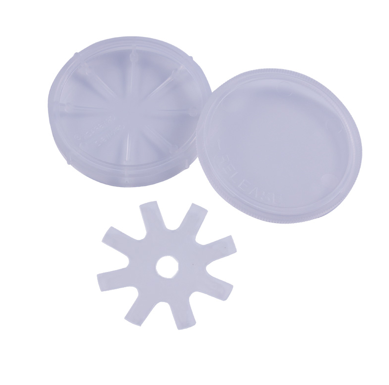
Cryspack’s wafer storage box is crafted to protect wafers of all sizes, from 75mm to 450mm. It is specially designed for applications where contact with the wafer’s top surface or edges must be avoided, making it ideal for storing diced wafers on film frames and handling delicate substrates such as InP, GaAs, AFM, and MEMs wafers. This design minimizes the risk of physical damage, ensuring that even the most fragile materials are secure during storage and transport.

A Solution for the Demands of R&D
For companies with active research and development departments, Cryspack’s wafer storage box offers flexibility and reliability. The product is specifically designed for high-frequency product iterations, allowing for rapid adaptation to different wafer sizes. This is particularly beneficial for companies like Cryspack’s customer, who frequently introduce new chip designs. By eliminating the need for customized waffle packs with each new design, Cryspack’s storage box provides a streamlined solution that reduces both lead times and costs.
Contamination Control and Electrostatic Discharge (ESD) Protection
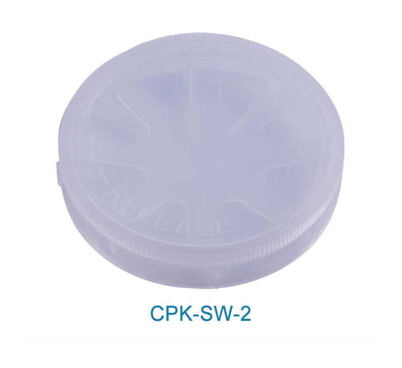
Cryspack’s wafer storage box is built from premium materials that guard against contamination and electrostatic discharge (ESD). Each box features a robust, dust-resistant design with a secure lid that creates a controlled environment for sensitive components. The anti-static properties of the material help prevent ESD, which is one of the leading causes of damage to electronic components during storage and transport.
The controlled environment in Cryspack’s wafer storage box reduces or even eliminates the need for additional cleaning steps, allowing companies to save time and reduce operational costs. For companies dealing with ultra-thin, high-value wafers, Cryspack’s solution offers a dependable way to preserve quality and protect yields.
Versatile Features and Applications
Single-Wafer Compartmentalization to Prevent Cross-Contamination
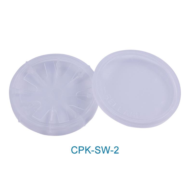
One of the standout features of Cryspack’s wafer storage box is its single-wafer compartment design. Each compartment holds only one wafer, effectively preventing cross-contamination between wafers. This design also minimizes handling risks, as each wafer remains securely in place within its compartment.
Space-Saving and Efficient Design for Improved Transport
With dimensions of Φ60mm x 12mm, Cryspack’s wafer storage box is optimized for space-saving storage and efficient transport. The compact design allows for easy stacking and organization, making it ideal for companies needing to maximize storage space in cleanroom environments.
Compatibility with a Range of Materials Beyond Silicon Wafers
While Cryspack’s wafer storage box is ideal for silicon wafers, it is also suitable for other materials, including quartz plates, glass sheets, sapphire plates, and gold-plated devices. This versatility makes it an invaluable solution for industries beyond semiconductors, such as optics and electronics.
Case Study: How Cryspack Helped a Semiconductor Giant Improve Yields and Reduce Scrap Rates
One of the world’s largest semiconductor companies, specializing in both analog and digital connectivity products, turned to Cryspack to address their wafer storage issues. This customer’s R&D center faced high levels of scrap and low yields due to chip migration and contamination. With IC chip sizes ranging from 1x1mm to 10x10mm, they required a flexible solution that could adapt to their rapidly changing product line.

After implementing Cryspack’s wafer storage box, the customer saw a dramatic reduction in yield loss. By using storage boxes that safely housed each IC chip individually, they eliminated the migration issues that had plagued their previous storage methods. Additionally, Cryspack’s contamination-resistant design reduced the need for extra cleaning steps, allowing the customer to speed up their production cycles and reach the market faster.
Why Cryspack is the Ideal Partner for Wafer Storage Solutions
Expertise in Customized Wafer Storage Solutions
Cryspack specializes in the manufacture of both standard and customized wafer storage boxes, providing tailored solutions for a variety of industries worldwide. They offer OEM and ODM services, allowing customers to obtain customized materials and equipment for their specific project needs. Cryspack’s team of professional engineers ensures top-tier technical support and customer service, making them a trusted partner for businesses facing complex storage challenges.
Fast Delivery and Rigorous Quality Assurance
Cryspack stands out for its commitment to quality and timely delivery. With normal delivery times within 20 working days, Cryspack often completes orders ahead of schedule, ensuring that customers receive their storage solutions when they need them. Before shipment, each product undergoes a 100% inspection process to ensure it meets Cryspack’s high standards.
Conclusion: Protect Your Wafers, Boost Your Yields
In the semiconductor industry, every wafer counts, and protecting them during storage and transport is essential for maximizing yields. Cryspack’s wafer storage boxes offer a comprehensive solution to the industry’s challenges, from device migration and contamination to electrostatic discharge and handling damage. With a design optimized for durability, contamination control, and ease of use, Cryspack’s wafer storage boxes are transforming the way companies manage their valuable wafers and substrates.
For companies looking to protect their investments, reduce yield loss, and improve operational efficiency, Cryspack provides reliable, flexible, and expertly crafted membrane box, gel sticky box, vacuum release tray, vacuum release box solutions. By choosing Cryspack, businesses can focus on what they do best—innovating—while knowing that their delicate wafers are safe and secure.

