Exploring Cryspack Wafer Boxes: Innovations in Semiconductor Packaging
2024.07.11 / By hqt
Cryspack, renowned for its cutting-edge solutions in semiconductor packaging, offers a range of wafer boxes tailored to meet the stringent demands of the industry. These boxes serve a crucial role in safeguarding delicate wafers and substrates during storage and transportation. Here’s an in-depth look at how Cryspack wafer boxes excel in protecting and preserving semiconductor materials.
Advanced Technology for Superior Protection
Cryspack wafer boxes utilize their proprietary Cryspack Vacuum Release® (VR) Technology, a hallmark feature shared with their VR trays. This technology is integral to maintaining the integrity of wafers ranging from 75mm to 450mm in size. Unlike traditional packaging methods, Cryspack’s VR Plates employ a unique Gel & Mesh surface on a flat plate, effectively cushioning and securing wafers without direct contact with their sensitive surfaces.
The VR Plates, available in brown phenolic (C) or transparent acrylic (T) materials, are designed with meticulous attention to detail. They prevent damage that could occur from surface contact or edge impact, crucial for fragile substrates like InP, GaAs, AFM, and MEMs wafers. Whether handling full wafers or diced components mounted on film frames, Cryspack wafer boxes ensure maximum protection throughout the supply chain.
Customization Options for Specific Needs
One of Cryspack’s strengths lies in its ability to customize wafer boxes according to specific client requirements. This flexibility is essential in an industry where diverse wafer sizes and handling specifications demand tailored solutions. Cryspack offers not only standard sizes but also designs and manufactures custom wafer boxes to accommodate unique dimensions and configurations.
Clients can choose between conductive black (C) or transparent (T) storage boxes, depending on their operational needs and preferences. Furthermore, Cryspack provides the option for custom prints such as grids, company logos, or other artwork, ensuring branding and identification needs are seamlessly integrated into the packaging.
Applications Across Semiconductor Industries
Cryspack wafer boxes find extensive application across various semiconductor sectors. They are particularly well-suited for environments where minimizing physical contact with wafers is critical. In research and development settings, where the integrity of materials can directly impact experimental outcomes, Cryspack’s VR Technology offers peace of mind by preventing inadvertent damage during handling and storage.
Manufacturers of semiconductor devices benefit from Cryspack’s solutions when transporting delicate substrates between different stages of production. The ability to transport 200mm and 300mm wafers mounted on film frames securely underscores Cryspack’s commitment to providing comprehensive solutions that address specific industry challenges.
Environmental Considerations and Sustainability
Beyond functionality, Cryspack also prioritizes sustainability in its manufacturing processes and product offerings. The materials used in their wafer boxes are chosen not only for their protective properties but also for their environmental impact. By employing durable and recyclable materials, Cryspack contributes to reducing the overall carbon footprint associated with semiconductor packaging.
Exploring Cryspack’s Wafer Boxes: Innovations in Semiconductor Packaging
Introducing Cryspack’s 6″*6″ Wafer/Large Format Acrylic Wafer Boxes
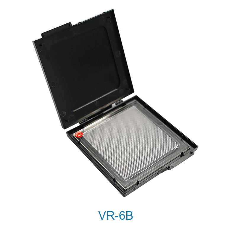
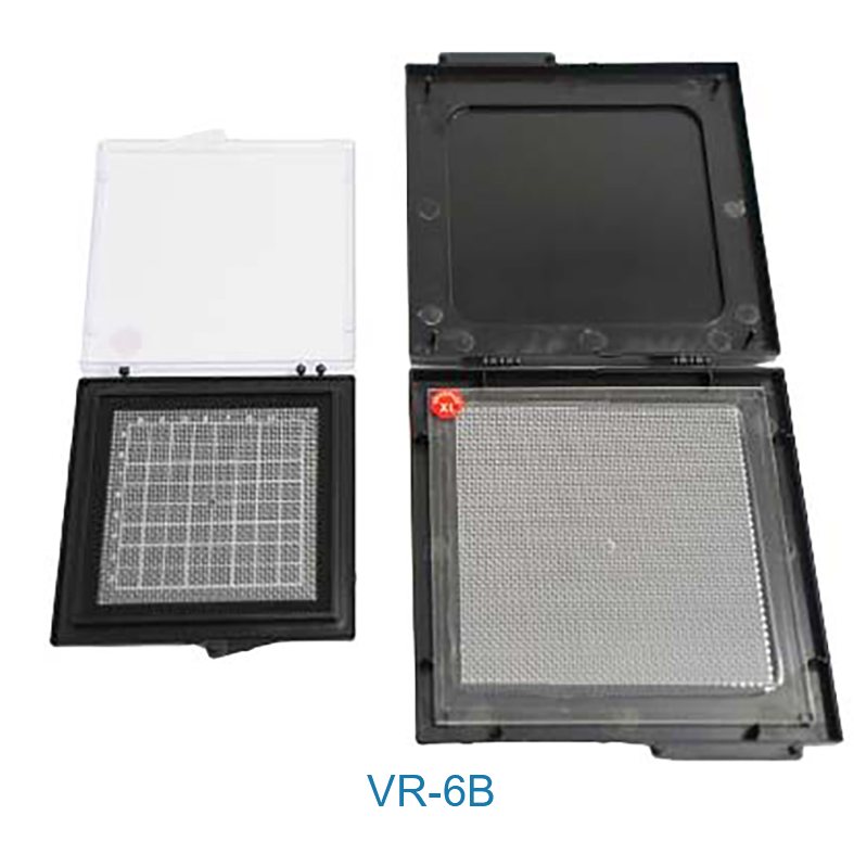
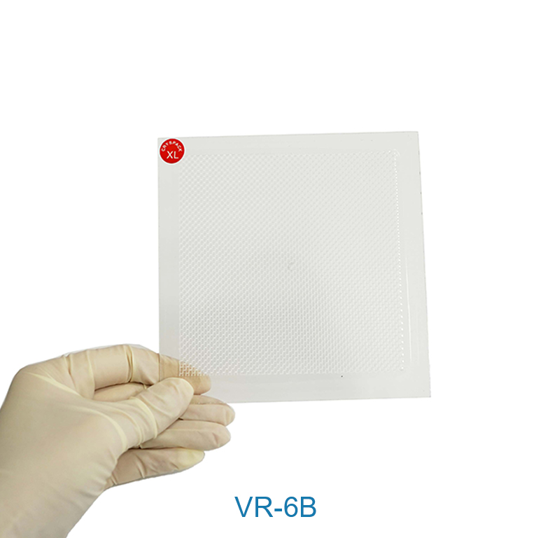
Cryspack, a leading manufacturer in semiconductor packaging solutions, has introduced an innovative line of 6″*6″ Wafer/Large Format acrylic wafer boxes designed to revolutionize the handling and transportation of delicate semiconductor and opto-electronic devices. These vacuum release (VR) plates are meticulously crafted to ensure the safe immobilization of fragile substrates during shipping, processing, and handling, making them indispensable across industries such as Semiconductor, Opto-electronics, and Telecommunication.
Innovative Vacuum Release Technology
Cryspack has pioneered a breakthrough in packaging technology with its Vacuum Release (VR) plates, which function akin to vacuum trays. These plates are specifically engineered to securely hold extremely fragile or thin devices like InP wafers, GaAs wafers, MEMs wafers, and AFM wafers. The VR plates excel in immobilizing these high-value substrates, offering unparalleled protection against damage and ensuring their integrity throughout the supply chain.
Specifications and Customization Options
The 6″*6″ Wafer/Large Format acrylic wafer boxes from Cryspack come with a range of specifications tailored to meet diverse industry needs:
Size and Standards: Available in 5 inch and 6 inch tray sizes, adhering to JEDEC standards.
Retention Levels: Offered in various gel tack levels—XL, L, M, H, HH—to accommodate different substrate requirements.
Mesh Geometries: Standard mesh size is 16, with options for other mesh geometries such as 33, 76, 103, 137, and 195 upon request.
Material and Customization: Manufactured from clear acrylic material, these VR plates can be customized with printed patterns to suit specific branding or identification needs.
Applications Across Industries
The versatility of Cryspack’s VR plates extends across several critical industries:
Semiconductor Industry
In the semiconductor industry, where the demand for precision and reliability is paramount, Cryspack’s VR plates play a crucial role. They ensure that delicate semiconductor wafers, such as Gallium Arsenide (GaAs) and Indium Phosphide (InP), are transported and processed without any compromise in their structural integrity. This capability is essential in maintaining yield rates and reducing production costs associated with damaged wafers.
Opto-electronics
Opto-electronic devices, which include components like lasers, LEDs, and optical sensors, often rely on wafer-level packaging to maintain performance standards. Cryspack’s VR plates offer a secure platform for these sensitive components, facilitating their safe transportation and handling from manufacturing facilities to assembly lines. The precise immobilization provided by the VR plates ensures that optical alignment and performance characteristics are preserved throughout the production process.
Telecommunication
In the field of telecommunications, where the demand for high-speed data transmission and reliable network infrastructure is ever-increasing, Cryspack’s VR plates contribute to the production of advanced components like MEMs (Micro-Electro-Mechanical Systems). These components are crucial for applications ranging from optical switches to signal processing devices. By safeguarding MEMs wafers during transit and assembly, Cryspack enhances the reliability and longevity of telecommunications equipment, thereby supporting the industry’s growth and innovation.
Advantages of Cryspack’s VR Plates
Cryspack’s 6″*6″ Wafer/Large Format acrylic wafer boxes offer several distinct advantages over traditional packaging methods:
Enhanced Protection: The VR plates provide superior protection against physical shocks and vibrations, safeguarding delicate substrates from potential damage during transit and handling.
Customization Capabilities: With options for custom print patterns and a variety of mesh geometries, Cryspack allows customers to tailor the VR plates to specific operational and branding requirements.
Cost Efficiency: By reducing the incidence of damaged wafers and ensuring higher yield rates, Cryspack’s VR plates contribute to overall cost savings in semiconductor manufacturing and other high-tech industries.
Conclusion: Choosing Cryspack for Superior Wafer Packaging
In conclusion, Cryspack stands out in the semiconductor packaging industry with its innovative wafer boxes that leverage advanced Cryspack Vacuum Release® Technology. These boxes are engineered to safeguard delicate wafers and substrates, ensuring they arrive at their destinations intact and ready for use. With customization options, robust protection capabilities, and a commitment to sustainability, Cryspack continues to be a preferred partner for companies requiring reliable semiconductor packaging solutions.
Whether you’re handling InP wafers in a research lab or transporting GaAs substrates in a manufacturing facility, Cryspack wafer boxes provide the assurance of quality and performance that today’s semiconductor industry demands. Explore the range of options available and discover how Cryspack can meet your specific packaging needs with precision and expertise.