Wafer Transportation: Addressing the Challenges with Advanced Wafer Container
2024.10.28 / By hqt
Have you ever considered the challenges of transporting delicate semiconductor wafers without damage? As the backbone of modern electronics, wafers are fragile, valuable, and prone to damage during handling and transportation. Ensuring their protection is critical to the efficiency of the semiconductor industry. Yet, the traditional packaging methods, like waffle packs, often fall short of providing the necessary protection. This blog delves into the current challenges in wafer transportation and how innovative solutions, such as Cryspack’s wafer containers, are revolutionizing the industry.

The Transportation Challenges of Semiconductor Wafers
Shrinking Die Size and Increased Vulnerability
As semiconductor technology advances, the size of the die continues to shrink, with thicknesses now often measured in tens of micrometers. Despite the increased performance and integration benefits, this miniaturization has created new challenges for the safe transportation and handling of wafers. Traditional packaging methods designed for thicker wafers, such as waffle packs, are no longer sufficient. The risk of die migration, where a die moves from one pocket to another during transportation, has become a costly and inconvenient issue.
This phenomenon, known as COOP (Component Out of Pocket), causes several problems:
Die damage from collisions: When dies migrate, they can collide, grind, or bounce against each other, leading to chipping or scratching.
Orientation errors: A die may flip or become lodged between pockets, causing errors in automated handling systems.
Costly rework and delays: Undetected die migration can lead to defective assembly, requiring expensive rework and troubleshooting.
The traditional wafer packaging systems were designed in an era when semiconductor dies were thicker and more robust. The introduction of thinner, more delicate wafers requires a new approach to packaging to prevent costly damage during transit.
Limitations of Traditional Waffle Packs
Traditional waffle packs, although widely used, are increasingly unsuited to modern semiconductor dies. The lack of adaptation to smaller, thinner wafers means that several issues arise during the transportation process:
Inadequate die protection: The old packaging was designed for thicker wafers, so thinner dies are not securely held in place, leading to die migration.
Lid warpage and deformation: The materials used in waffle pack lids, such as polypropylene or polycarbonate, are prone to warping, especially under pressure. This warpage creates escape paths for a die, increasing the risk of COOP.
Electrostatic discharge (ESD): Traditional packaging often lacks sufficient protection against ESD, a significant risk factor for sensitive semiconductor components.
The root causes of die migration are varied, including lid warpage, operator errors, and worn clips used to secure the trays. Without a comprehensive solution, manufacturers face increased costs due to damaged components, reduced machine utilization, and additional quality control processes.
The Need for Updated Wafer Container
Why Traditional Packaging Needs an Upgrade
With the increasing fragility of semiconductor dies, the need for updated packaging solutions is more pressing than ever. Traditional waffle packs have proven inadequate for several reasons:
Structural limitations: The design of waffle packs has not evolved alongside wafer technology, leaving critical gaps in protection.
Increased handling risks: Opening and closing waffle packs can cause die movement, leading to further damage.
Time-consuming inspection: COOP increases the need for post-transportation inspection, adding to labor costs and production delays.
The rise of more advanced wafers requires a modern packaging system that can fully protect the die throughout the supply chain, from the manufacturer to the end user.
Wafer Container Solutions: How They Address Key Problems
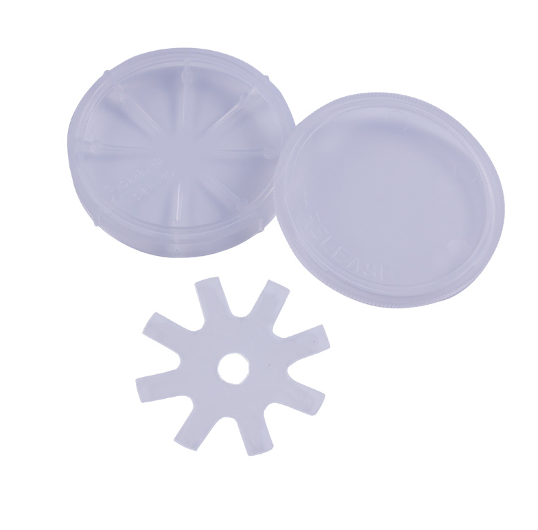
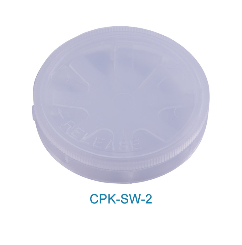
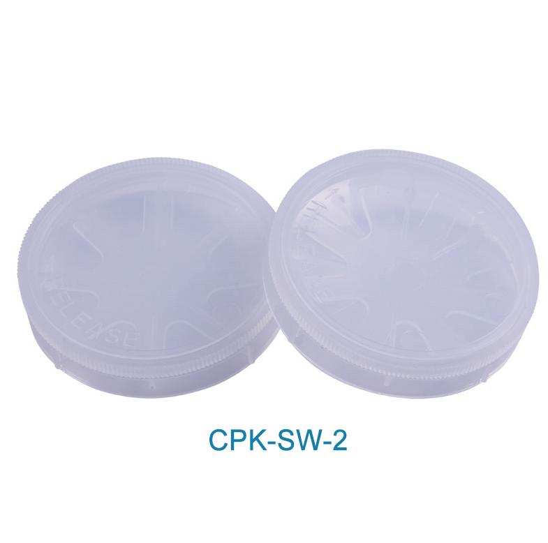
Cryspack, a leader in precision packaging solutions, has responded to these challenges with innovative wafer container designs. These containers are built with cutting-edge materials and engineered to address the vulnerabilities of traditional systems. Here’s how they solve the critical issues faced during wafer transportation:

Secure Encapsulation of Each Wafer: Cryspack’s wafer containers ensure that each wafer is fully secured, preventing die migration. The containers use a specialized design to keep each die in place during packing, shipping, and unpacking. This minimizes the risk of COOP, reducing damage and the need for costly rework.
Enhanced Material for Protection: The containers are made from low outgassing, static dissipative polyurethane foam, which is integrated with an industry-approved interleaf material. This construction not only protects wafers from physical damage but also shields them from ESD, a common issue in semiconductor transportation.
Warpage Prevention and Uniform Compression: One of the most significant improvements in Cryspack’s design is the introduction of a new clip system that provides uniform compression around the entire lid perimeter. This tight seal ensures that even warped trays do not create escape paths for the dies. The materials and design also prevent the deformation of the lids and trays during transit.
The Benefits of Modern Wafer Containers
Reducing Manufacturing Costs and Increasing Efficiency
By eliminating the risk of die migration, Cryspack’s wafer containers help reduce manufacturing costs in several ways:
Fewer damaged components: The robust design prevents wafer damage, reducing the need for rework and saving on the cost of replacement parts.
Improved production flow: With fewer defects and less downtime, manufacturing lines can operate more efficiently, resulting in higher machine utilization and faster production times.
Enhanced quality control: The need for post-transportation inspections is minimized, allowing manufacturers to focus resources on value-adding processes.
Optimizing Handling and Transportation
Cryspack’s wafer containers are designed for easy handling and transportation. The compact and lightweight format allows for space-saving storage and increased transport efficiency. The secure lid ensures that wafers remain in place throughout the journey, eliminating the need for frequent checks or adjustments.
Moreover, the containers are versatile, allowing for the storage and transport of not only semiconductor wafers but also other sensitive components like sapphire plates and gold-plated devices. This flexibility makes them an ideal choice for companies involved in the optics, electronics, and semiconductor industries.
ESD Protection and Compliance with Industry Standards
One of the standout features of Cryspack’s wafer containers is their ESD protection. The materials used in these containers are tested to ANSI/ESD standards, ensuring that sensitive wafers are protected from electrostatic discharge during transportation. This is crucial for high-value semiconductor components, which can be easily damaged by even the smallest ESD event.
Additionally, Cryspack’s containers meet EU ROHS and REACH certification standards, making them compliant with industry regulations and environmentally friendly.

Cryspack: Leading the Future of Wafer Packaging
Cryspack has established itself as a trusted provider of innovative packaging solutions such as membrane boxes, gel sticky boxes, vacuum release trays, and vacuum release boxes, with over 1,000 customers worldwide. Their commitment to quality and innovation is evident in their advanced wafer container designs, which address the pressing challenges faced by the semiconductor industry today. By offering custom services and reliable products, Cryspack ensures that their customers can safely transport even the most delicate and valuable semiconductor components.
Conclusion
The increasing complexity and fragility of semiconductor wafers require a new approach to transportation and storage. Traditional waffle packs are no longer sufficient to meet the demands of modern manufacturing processes. Cryspack’s wafer containers provide the solution, offering superior protection, ESD safety, and efficient handling. For companies looking to reduce costs, minimize damage, and increase production efficiency, Cryspack’s innovative containers are the key to staying ahead in the fast-paced semiconductor industry.

