Wafer Transportation: The Ultimate Wafer Shipping Box Solution
2024.09.25 / By hqt
Are you constantly frustrated by the recurring issue of semiconductor devices sustaining damage during transit? Finding yourself grappling with the challenge of discovering a dependable method to preserve the integrity of your valuable wafers? If so, the solution is at hand. The Cryspack wafer shipping box presents itself as a state-of-the-art innovation, engineered specifically to accommodate even the most fragile wafers and semiconductor substrates with an extraordinary level of care and precision. Yet, what is it that truly distinguishes this product in the competitive realm of wafer transportation and storage?
Ensuring Superior Protection: Advanced Vacuum Tray Technology
Exceptional Device Safeguarding
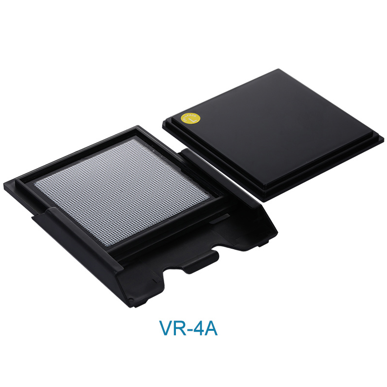
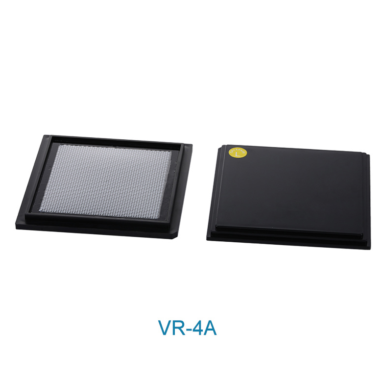
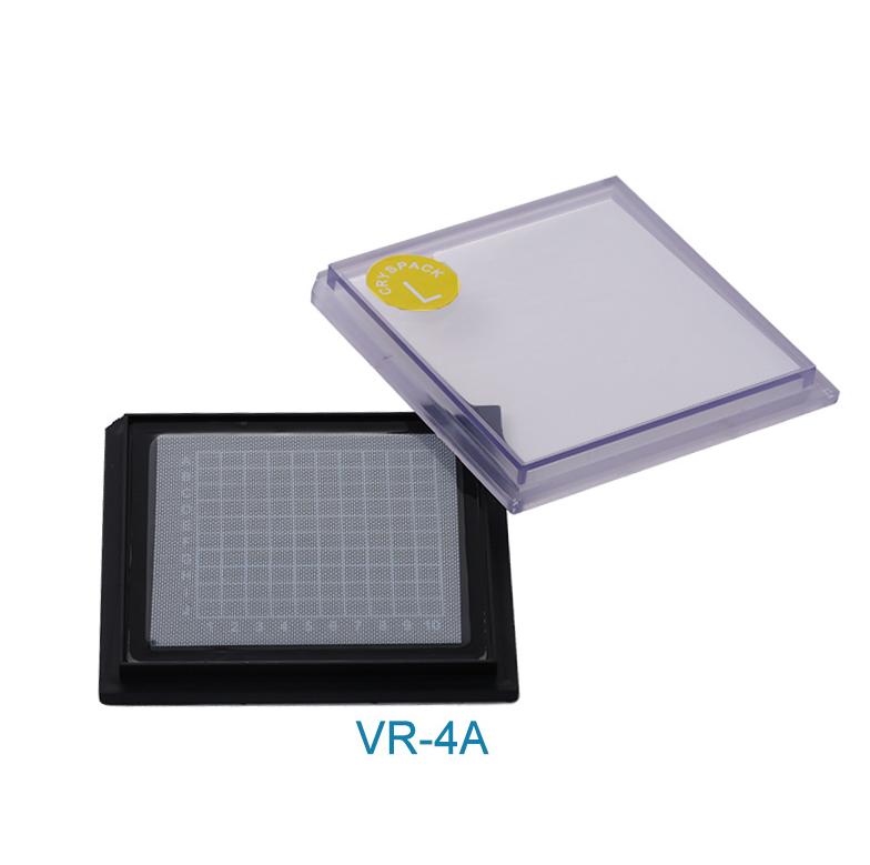
At the core of Cryspack wafer shipping boxes lies the integration of pioneering vacuum tray technology, a system that delivers dynamic retention, effectively guaranteeing that wafers remain firmly secured during the entire transport process. This patented mechanism immobilizes the wafers, offering the unique advantage of doing so without exerting undue pressure on their sensitive surfaces or edges. Whether your concern is the transportation of fully intact wafers, partially processed ones, diced wafers, or highly fragile and valuable substrates like InP, GaAs, or MEMs wafers, this highly developed system offers comprehensive protection, shielding these devices from the dual threats of physical damage and contamination.
Tailored Solutions for Every Wafer Dimension
From the smallest 75mm wafers to the largest 450mm substrates, Cryspack offers an impressive range of customizable configurations. These flexible options allow you to choose the most suitable tray size, retention level, and mesh geometry for your specific needs. By precisely tailoring the configuration to match your wafer’s dimensions, the system significantly reduces movement during shipping, thereby offering a heightened level of protection against the risks posed by unwanted shifts, impacts, or other transportation hazards.
Enhanced Protection Against Particulates
An additional and crucial benefit of Cryspack’s vacuum tray technology lies in its ability to provide superior protection against particulates. Given the high sensitivity of semiconductor devices to contamination, even minute particles can severely impair performance and compromise overall yield. The isolation created by the vacuum system serves as a robust barrier against such contaminants, drastically lowering the likelihood of particle intrusion into the container. This ensures that your wafers remain pristine, preserving their quality and maintaining their original condition throughout the entire shipping process.
Streamlining Operations with Efficient Handling
Faster Production Cycles
Cryspack’s wafer shipping box is engineered for operational efficiency. By minimizing the amount of human handling required, the vacuum technology facilitates quicker placement and retrieval of wafers, shortening production cycles. This not only boosts productivity but also significantly reduces labor costs, as fewer resources are needed to manage the wafers during transportation and storage.
Reducing Downtime
Efficient handling also means less downtime due to accidents or misplacements. With the Cryspack system, wafers are easy to insert and retrieve, reducing the likelihood of errors or mishandling. This increased operational fluidity allows for faster workflows, ensuring that your production processes remain uninterrupted and efficient.
Data-Driven Design for Reliability
Cryspack’s wafer shipping boxes are the result of extensive testing and analysis. Each box is designed with a focus on high performance and reliability, allowing semiconductor manufacturers and researchers to trust that their devices are being transported under optimal conditions. The data-driven design ensures that the boxes meet rigorous industry standards, providing peace of mind when it comes to product integrity.
Key Applications of Wafer Shipping Box
Semiconductor Manufacturing
For manufacturers in the semiconductor industry, the Cryspack wafer shipping box provides a vital layer of protection. Silicon wafers go through numerous processes during their creation, from slicing and polishing to lithography and doping. At each stage, they are vulnerable to damage, whether from physical impacts or contamination. Cryspack’s robust design ensures that wafers are shielded from these hazards, enabling manufacturers to deliver high-quality products consistently.
Research and Development
In research and development settings, where sensitive prototypes and experimental wafers are being created, the last thing a team wants is for their hard work to be compromised due to improper handling. The Cryspack wafer shipping box offers R&D teams the reliability they need to transport and store their valuable research wafers without worry. The vacuum retention system ensures that even the most fragile wafers arrive intact and uncontaminated.
Chip Transport and Storage
When it comes to transporting semiconductor chips, the risk of damage is high, especially for fragile or valuable devices. The Cryspack wafer shipping box mitigates this risk by providing a secure environment that shields the chips from external forces. This makes it the ideal solution for transporting high-value parts. Additionally, its storage capabilities extend the lifespan of wafers, making it a cost-effective way to store silicon chips and other semiconductor components for extended periods.
Advantages of Cryspack Wafer Shipping Boxes
Improving Yield and Reducing Loss
One of the most significant advantages of using Cryspack wafer shipping boxes is the protection they offer against wafer breakage, contamination, and degradation. By safeguarding wafers from these common issues, the boxes help to improve overall yield and reduce the need for costly rework. This means fewer rejected wafers, less waste, and a more streamlined production process.
Enhancing Operational Efficiency
Cryspack’s wafer shipping boxes not only protect your devices but also contribute to overall operational efficiency. By reducing handling time and minimizing human error, these boxes allow your team to work more productively. This enhanced efficiency leads to increased output, better quality control, and significant cost savings over time.
Risk Management and Reliability
When dealing with high-value semiconductor devices, the risk of loss due to transportation or handling errors can be considerable. Cryspack’s wafer shipping boxes are designed with risk management in mind, offering an added layer of security that protects against transport-related damage. This not only helps to preserve product quality but also reduces the financial impact of potential product loss, giving you greater control over your business operations.
Configurable Wafer Shipping Solutions
Standard Tray Sizes and Retention Levels
Cryspack offers a wide range of tray sizes to accommodate various wafer dimensions, from 2 inches to 6 inches, all based on JEDEC standards. The availability of different retention levels—XL, L, M, H, and HH—ensures that you can choose the optimal configuration for your specific needs, ensuring that your wafers remain immobilized during transport without the risk of damage from excessive pressure.
Multiple Mesh Geometries for Precise Customization
In addition to tray sizes and retention levels, Cryspack provides a variety of mesh geometries, ranging from 16 to 195. This level of customization allows you to fine-tune the shipping box to meet the sensitivity of your wafers, ensuring that they remain secure while minimizing the risk of contamination or damage.
Custom Print Patterns for Branding
For wafer wholesalers and dealers looking to add a personal touch, Cryspack’s wafer shipping boxes can also be customized with print patterns. This allows businesses to not only protect their products but also to showcase their branding, adding a level of professionalism to their packaging that can set them apart from the competition.
Conclusion: Elevating Wafer Transportation to the Next Level
In the world of semiconductor manufacturing, research, and chip transport, ensuring the safe handling of wafers is crucial to maintaining product quality and minimizing costs. Cryspack wafer shipping boxes offer a comprehensive solution to the challenges of wafer transport and storage, combining cutting-edge vacuum tray technology with customizable features that make it the perfect choice for a wide range of applications.
Whether you are a manufacturer, researcher, or wholesaler, Cryspack’s wafer shipping box can help you streamline your operations, reduce risk, and improve the overall quality of your semiconductor products. With this solution, wafer handling becomes more efficient, reliable, and secure—protecting your investment every step of the way.
By choosing Cryspack, you’re not just investing in a shipping box—you’re investing in the future of your business.