Handling Wafer VR Plates for the Semiconductor Industry
2024.09.24 / By hqt
What Measures Are in Place to Safeguard Fragile Wafers?
Within the highly specialized domain of semiconductor manufacturing, one of the most intricate and pressing issues revolves around the proper handling of sensitive wafers. Even the most minimal scratch, hairline crack, or minor defect can compromise an entire wafer, resulting in substantial financial losses. Consider, for instance, wafers crafted from highly delicate and brittle materials such as Indium Phosphide (InP), Gallium Arsenide (GaAs), or Micro-Electro-Mechanical Systems (MEMS) wafers—each wafer, depending on its composition and intended application, can be valued at several thousand dollars. The question thus arises: how can such costly and sensitive substrates be adequately protected during their various stages of storage, transportation, and processing?
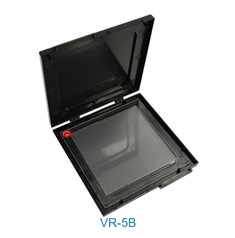
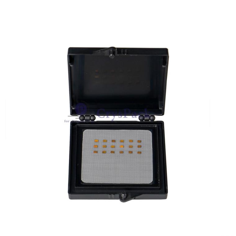
The answer lies in the innovation of Wafer VR Plates, specifically engineered to offer the highest degree of safeguarding for these vulnerable materials. Designed with precision, these plates are tailored to meet the stringent demands of industries where contact with the wafer’s sensitive top surface or its fragile edges must be meticulously avoided. This essential solution is brought to the market by Fuzhou Cryspack Opto-Electronic Technology Co., Ltd., a renowned leader in the development of wafer handling technologies. Their Acrylic Wafer VR Plates are adeptly constructed to accommodate wafers and substrates of varying sizes, from smaller units measuring 75mm up to larger substrates reaching dimensions of 450mm. In environments where wafer integrity is paramount, these protective plates have become indispensable tools for ensuring safety and precision.
By offering unparalleled protection and reducing the risk of contamination or damage, these VR plates have redefined the standards of wafer management, contributing to the seamless operation of semiconductor manufacturing processes.
Advanced Features of Wafer VR Plates
1. Industry Standardized for Reliable Precision
When it comes to handling wafers, precise dimensionality and compatibility with industry standards are crucial. Wafer VR Plates are built to meet and exceed these strict requirements, making them a reliable choice for any semiconductor operation.
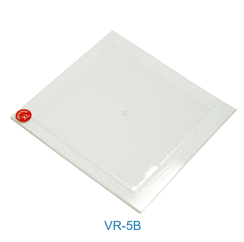
These carriers are made specifically for 5-inch wafers, ensuring that they conform to the most dependable industry benchmarks. Whether you are working with diced wafers on film frames or large substrates, these carriers offer the versatility and reliability you need. The customizable features of these plates make them adaptable for various wafer types, providing a tailored solution for every application.
2. Chemically Resistant Adhesive for Customization
One of the standout features of the Wafer VR Plates is the chemically resistant adhesive that allows for easy customization. This adhesive ensures that the plates can accommodate different gel tack levels (XL, L, M, and H), depending on the specific wafer type. This adaptability makes the plates suitable for a wide range of applications, from handling thin, high-value substrates to protecting more robust materials.
Having the ability to choose different adhesive strengths ensures that wafers remain securely in place, reducing the risk of damage during handling, transport, or storage.
3. Variable Mesh Selection for Multiple Wafers
The variable mesh selection feature is another unique selling point of the Wafer VR Plates. This allows users to choose from a wide range of mesh sizes that can fit single or multiple wafer types. Whether you’re handling InP wafers, GaAs wafers, or AFM wafers, the customizable mesh selection ensures that you have the right fit every time.
By offering this level of flexibility, Wafer VR Plates make it easier for semiconductor companies to streamline their processes, improve productivity, and reduce the risks associated with wafer handling.
Versatile Applications of Acrylic Wafer VR Plates
1. Safe Wafer Storage
One of the most critical stages in the wafer lifecycle is storage. Improper storage conditions can lead to wafer contamination, physical damage, or even chemical degradation. Wafer VR Plates are specifically designed to provide a controlled environment for storing 5-inch wafers. The acrylic material used in these plates is both robust and crystal clear, ensuring that the wafers remain visible for inspection while being stored safely.
With their ability to maintain the integrity of wafers during storage, these plates are a key tool in ensuring that delicate materials remain in optimal condition before they are needed for processing or testing.
2. Efficient Wafer Transfer
In semiconductor manufacturing, transferring wafers between different stages of the production process is a delicate task. Wafer VR Plates provide a safe and stable solution for wafer transfer, ensuring that these fragile materials are not exposed to unnecessary risks.
Whether wafers are being transported across a cleanroom or moved from one machine to another, the VR Plates offer a protective barrier that prevents any contact with the top surface or edges of the wafers. This level of protection is essential in reducing breakage and ensuring that the wafers arrive at their destination intact.
3. Stability During Wafer Processing
Processing wafers often involves exposure to chemicals, extreme temperatures, and mechanical stress. Wafer VR Plates are designed to withstand these challenges by providing a stable platform during wafer processing. The chemically resistant properties of the plates ensure that they can be used in environments where exposure to harsh substances is a concern.
In addition to their stability, the clear acrylic material of the plates allows for easy inspection of the wafers during processing. This transparency ensures that operators can monitor the condition of the wafers in real-time, reducing the risk of processing errors.
Why Choose Acrylic Wafer VR Plates?
1. Maximum Protection for High-Value Wafers
When it comes to wafer protection, the patented design of the Wafer VR Plates offers unparalleled defense against breakage. Fragile wafers made from materials like InP and GaAs require extra care, and these plates are specifically built to meet that need.
The advanced acrylic construction not only provides a durable and sturdy platform but also prevents any direct contact with the wafer surface or edges. This design feature significantly reduces the risk of damage, making Wafer VR Plates an essential tool for anyone working with high-value wafers.
2. Increased Productivity through Configurability
Semiconductor manufacturing is a highly competitive industry where productivity is paramount. Wafer VR Plates help to streamline wafer handling processes by offering customizable solutions tailored to specific needs. From selecting different adhesive tack levels to choosing the appropriate mesh size, these plates allow operators to configure the product based on the unique requirements of their wafers.
This level of customization not only increases productivity but also reduces the likelihood of handling errors, leading to more efficient operations overall.
3. Unrivalled Industry Knowledge and Expertise
When you choose Wafer VR Plates from Fuzhou Cryspack Opto-Electronic Technology Co., Ltd., you’re tapping into years of experience in the wafer handling industry. Their extensive knowledge in developing reliable wafer management solutions is reflected in the quality and durability of their products.
Whether you’re looking to protect wafers during transport, processing, or storage, their expertise ensures that you receive a product that is built to last and perform at the highest level.
The Future of Wafer Handling
As technology continues to evolve, the demand for high-quality wafer handling solutions will only increase. Wafer VR Plates are at the forefront of this innovation, providing a solution that not only protects fragile wafers but also enhances productivity and reduces costs. With the ability to customize the plates to meet specific needs, semiconductor manufacturers can rest assured that their wafers are in safe hands.
By choosing Wafer VR Plates from Fuzhou Cryspack Opto-Electronic Technology Co., Ltd., companies are investing in a product that is built to last and engineered to protect their most valuable assets. Whether for research and development, wafer transfer, or storage, these plates offer the highest level of protection and reliability in the industry.
Conclusion
In conclusion, Wafer VR Plates provides a comprehensive solution for handling fragile wafers, ensuring maximum protection and efficiency throughout every stage of the wafer lifecycle. For companies in the semiconductor industry, investing in these advanced acrylic plates is a smart choice that guarantees long-term savings and peace of mind.